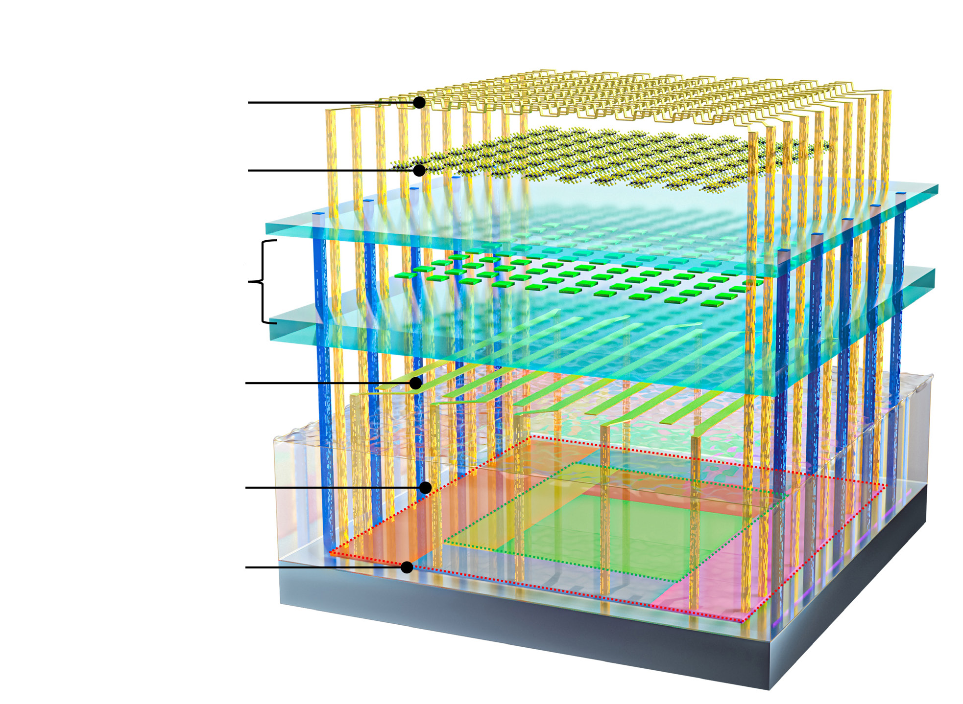
Confronted with the fundamental challenge of Moore’s Law approaching its physical limits, two-dimensional semiconductors with thicknesses of only one to three atomic layers are internationally recognized as a key pathway to technological breakthrough. Both industry and academia are striving to validate the advantages of two-dimensional electronics through heterogeneous system integration. However, the atomic structure of two-dimensional semiconductors is as thin and fragile as cicada wings, making large-scale integration extraordinarily challenging.
This research achieves a full-chain breakthrough from fundamental device mechanisms in two-dimensional electronics to engineered system-level integration through atomic-scale fabrication technology (ATOM2CHIP). Its technological blueprint encompasses full-stack on-chip integration processes and cross-platform system design, enabling atomic-scale “conformal adhesion” integration between two-dimensional semiconductors and CMOS chiplets, as well as monolithic high-density interconnection and protocol-based communication within heterogeneous circuits. The research pioneers the two-dimensional semiconductor/ silicon hybrid architecture (“Changying”) flash memory chip, which is a high-complexity, instruction-driven, fully functional chip supporting 8-bit instructions and 32-bit parallel processing, with an integration yield as high as 94.3%.
This achievement is supported by complete independent intellectual property rights in China and establishes a new paradigm for atomic-scale chip integration.
Main contributors: ZHOU Peng, LIU Chunsen
Main supporting institution: Fudan University