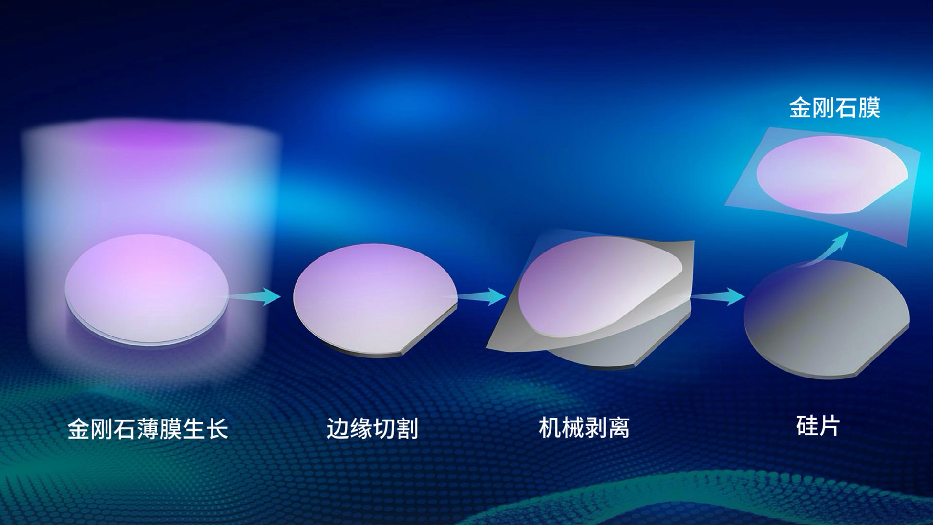
Diamond is hailed as the “ultimate semiconductor material” due to its exceptional hardness, ultrahigh carrier mobility, high dielectric breakdown strength, outstanding thermal conductivity, and wide bandgap characteristics, exhibiting transformative potential across numerous fields. However, traditional fabrication techniques are almost incapable of producing large-scale, ultra-thin diamond films, severely restricting its industrialization process.
This research has developed an “edge-exposed exfoliation” method by modeling the asymmetric nature of defects at the as-grown and buried surfaces of the membrane, which can achieve scalable production of inch-scale flexible, ultrathin, ultraflat diamond films using a “one-step process”. By optimizing peeling angle and thickness parameters through theoretical modeling, this method accomplishes in seconds what traditional techniques such as laser slicing or substrate etching require tens of hours to complete, significantly improving production efficiency and reducing costs. The resulting sub-micron-thick diamond membranes feature surface roughness below the nanometer scale and can be bent in 360 degrees. Their ultraflat surfaces are fully compatible with existing semiconductor CMOS processes, and their flexibility paves the way for applications like “elastic strain engineering” and “strain sensing”, which is unattainable with conventional rigid diamond bulk materials.
This method is expected to accelerate the application of diamond membranes in next-generation high-performance electronics, flexible optoelectronics, quantum technologies, and related fields.
Main contributors: CHU Zhiqin, LIN Yuan, LI Kwai Hei, WANG Qi
Main supporting institutions: The University of Hong Kong; Southern University of Science and Technology; Dongguan Institute of Opto-Electronics Peking University